Usually, the Fermi level, eF, is calculated from the majority-carrier concentration. The process is explained in the Mechanisms section. But, also, the minority-carrier concentration can be found from Fermi level:
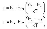
Where:
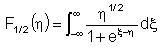
Intrinsic carrier concentration is defined as follows:
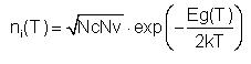
Where:
Intrinsic electronic level is defined as follow:
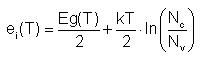
Where:
DADOS implements two parameters depending on the charge:
Where:
This probability is calculated using the expresions shown in the concentration ratio of charged species section.
The formation energy for a species "X" with charge "j" is given by:
![]()
Where:
Formation energy for vacancies is plotted in dashed lines in the figure below. The total effective formation is the lowest one. That is given by:
![]()
Where:
Solid lines represent the activation energy of DC* product of charged species.
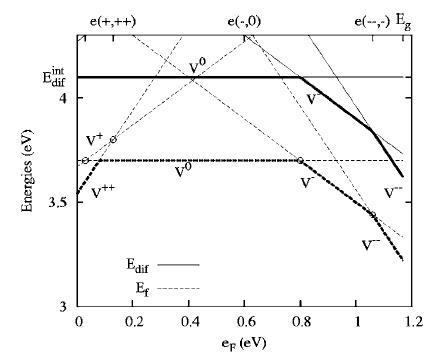
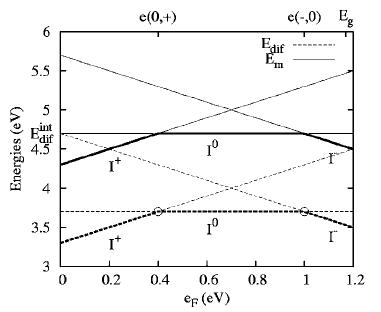
The situation for interstitials is analog.
The relation between the electric field (F) and the Fermi level (eF) is:

And, also, the relation between the formation energy (Ef) and the electric field (F) is:
![]()
The figure below shows electric drift as a natural consequence of the local dependance on the formation energies of charged particles.
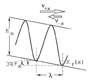
The relation between the migration frequency in the positive and negative directions along the x axis for a point defect with charge "jq" is (assuming constant band gap):
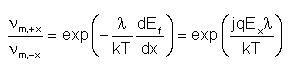
where:
Let's suppose this structure:
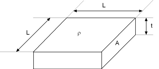
As its top surface is square, we can define the sheet resistance as follows:
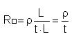
Where
In an electronic device, under extrinsic conditions, the sheet resistence can be approximated by:
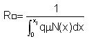
Where:
For a given diffusion profile, sheet resistance is uniquely related to the surface concentration of the diffused layer and the background concentration of the wafer.