Motivation / history
Why to design a 1 MHz 6502
computer during 2010? Some nostalgia is involved, sure. It is also
something that I got posponed since long time ago. Back, in the old
days, I had a little consideration for the 6502. I always regarded
it as inferior to its main competitors, mainly the Z80. Therefore, I
built several computer prototypes around the Z80 and never paid
attention to the 6502. Then, it came the time for more powerful
computers and I turned towards the 68000. Later, the microcontrollers
offered a complete computer in a single chip. No more routing of
address and data buses! Just an IC and a quartz crystal and that's
all (and, today, not even the crystal is needed). As a consequence, I
got a handful of old ICs rusting in drawers for 20 years.
I changed my point of view about
the 6502 after I tried to design a CPU core by myself. At that time
I also knew the ARM architecture, and I started to recognize the
value of hardware efficiency: do more with less transistors and less
watts. Squeeze it into a small chip area, and sell it really cheap,
and this was what Chuck Peddle, the designed of the 6502, indeed
did. The amazing aspect of the 6502 was its price. It was so cheap
that engineers first though it was a joke. Soon after the 6502 found
its way into a lot of personal computers, arcade games and so on.
So, I made up my mind to design
and build a computer prototype around this CPU. First, I started
with an ambitious design. It included up to 4Mb of dynamic RAM, a
crude MMU with 16kB pages, and even a protection mechanism against
the bad behavior of user tasks: If a IRQ was left unserviced for too
long an NMI was triggered. The MMU will restrict the I/O accesses to user tasks anyway. I also started to write a multitasking
system using a self made emulator for the prototype to come... But,
then I learned about the KIL
op-codes.
These op-codes can stop the
processor completely, and there is no protection against them. I guest the 6502 never went into space because of this. So,
the whole design was more or less pointless. Also, the layout of the
prototype turned out to require a lot of space, more than the usual
boards I was using.
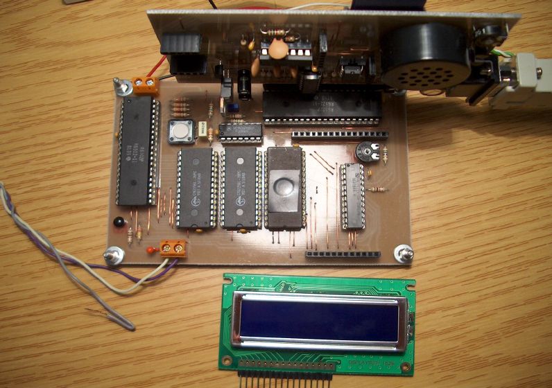
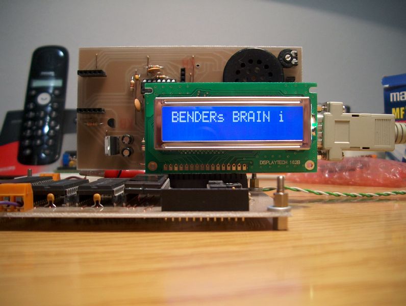
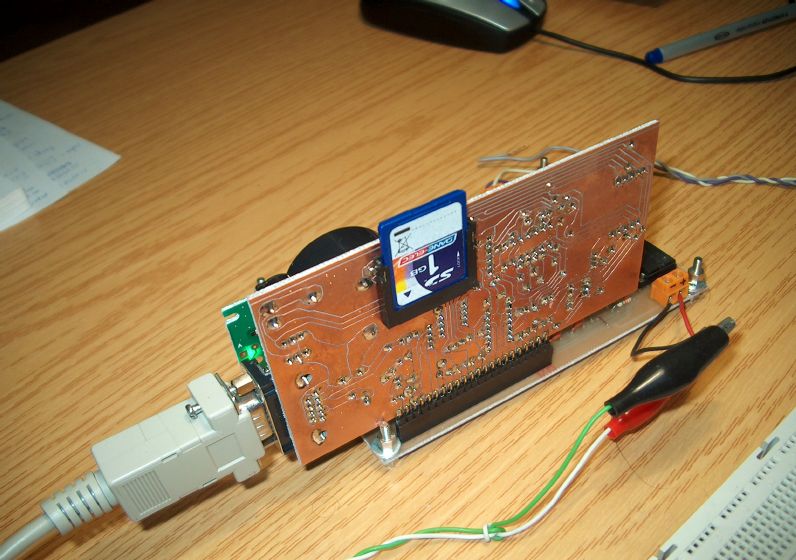
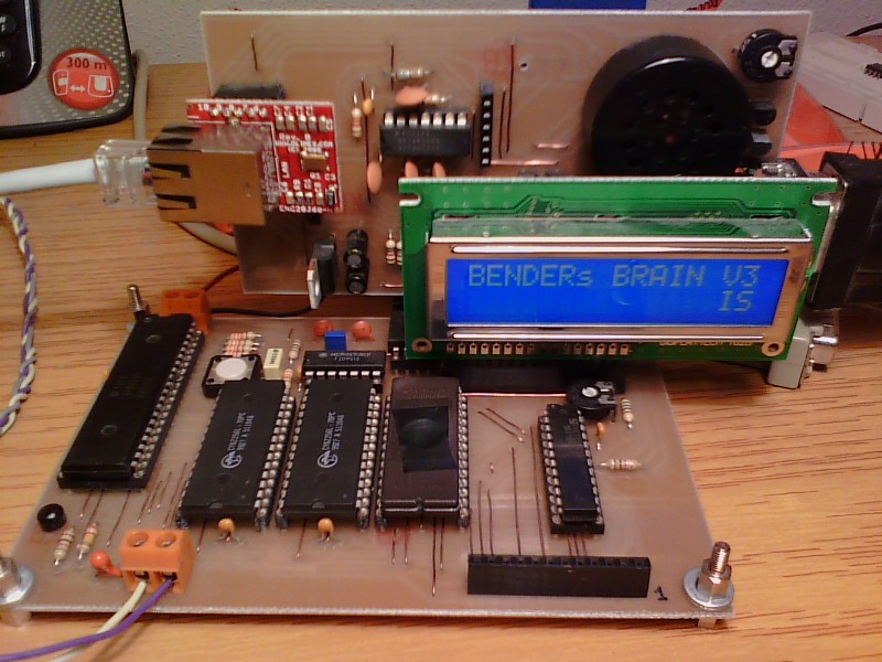
At the end I settled for a
simpler design. A little more than the usual 6502 + VIA SBC. Later, I
added a peripheral card with some interfaces to the VIA.