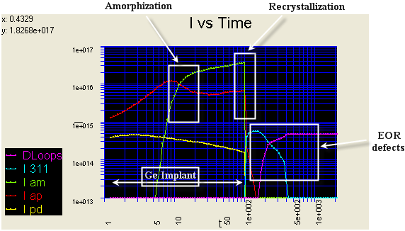
In this simulation, a Si amorphous layer is formed by Germanium implant. Subsequent annealing at 800 °C causes the recrystallization of the amorphized region and the evolution of the End of Range (EOR) Defects. Ge is implanted at 20 keV with a dose of 9 x 1013 cm-2 and a dose rate of 1 x 10¹² ions cm-2 s-1.
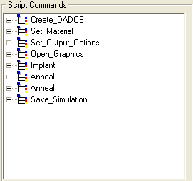
A name must be assigned to Object Name and Client Data.
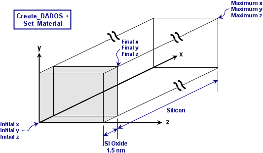
Maximum x: 350 nm
Maximum y: 80 nm
The values of the parameters Minimum x, Minimum y and Minimum z must be zero.
Material: SiOxide
Initial x: 0
Initial y: 0
Initial z: 0
Final x: 1.5 nm
Final y: 10000 nm
It is important to point out that the values of Final y and Final z are greater than the values of Maximum y and Maximum z in Create_DADOS command. In this way, the new material layer fits the previously defined simulation box. In this case, a thin layer of Silicon Oxide with a thickness of 1.5 nm on top of the Si is included.
After these two commands, the following simulation box has been created:
Start Output Time (s): 1 s
Snapshots per Decade: 30
UVAS starts the graph structure defined in the GPH file. As the simulation proceeds, UVAS takes different snapshots and the results are plotted on the screen.
Implant species: Germanium
Energy (keV): 20 keV
Tilt: 7°
Rotation: 45°
Dose: 1 x 1015 cm-2
Dose rate: 1 x 10¹³ ions cm-2 s-1
Target Structure: Crystal
Initial Temperature: 26.85 °C
Final Temperature: 800 °C
Initial Temperature: 800 °C
Final Temperature: 800 °C
Time: 2000 s
Ge implant produces damage accumulation until a continuous amorphous region is formed. Point defects produced by Ge implant form amorphous pockets. When in a zone the damage density is high enough, this zone is considered amorphous. In the graph below, a continuous amorphous region of about 60 nm thick appears before 9 seconds from the beginning of the implantation.
During annealing, recrystallization of the amorphized region takes place. The amorphous/crystalline interface moves towards the surface until all the previously amorphized silicon is converted in crystalline. This recrystallized Si region is defect-free. On the other hand, the region beyond the initial position of the amorphous/crystalline interface is damaged, but not amorphized. The high concentration of defects in that zone gives rise to the formation first of {311} and dislocation loops. Defects in this region are called End Of Range (EOR) defects. Evolution of this EOR defects is to be discussed.
Simulation evolution is shown in the following graph.
The simulation can be divided in the following moments:
First of all, Ge is implanted in order to amorphize part of the silicon bar. In this way, it is possible to study two physical mechanisms: amorphization and recrystallization.
The atomic mass of Ge is much greater than that of the Si. This implies that Ge causes much damage during the implantation. The 20 keV Ge implant creates a high concentration of interstitials and vacancies very quickly. Consequently, gives rise to a region which damage is above the amorphization threshold level, and therefore, is considered amorphous.
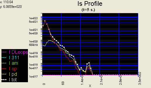
As implant proceeds, the concentration of interstitials in amorphous pockets is increasingly high and the damage of the region next to the surface increases considerably. The interstitials profile at 5 s is shown in the following graph:
![]()
The amorphization threshold is a simulation parameter (defined in the file "dados.ddp") which indicates the concentration of interstitials and vacancies from which Si amorphizes. For this simulation, the value of the parameter AmorphizationThreshold is 2.2 x 10²² (I+V) cm-3.
Next graphs show the evolution of amorphous regions.
Approximately at 6 s of Ge implantation, damage concentration has increased so some amorphous regions are formed along the sample. First, the amorphized region is close to the surface. When Ge implant continues, the amorphization spreads and more amorphous regions appears.

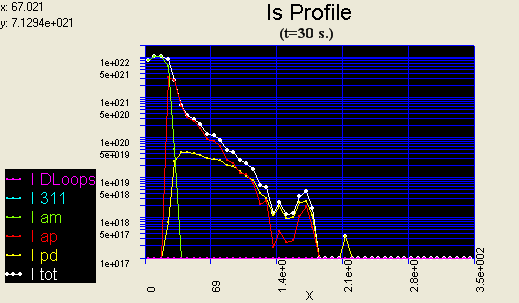
Overlapping of the subsequent Ge cascades produces more damage accumulation, until finally a continuous amorphous region appears. Therefore, point defects in the existing amorphous pockets in that region become part of the Si amorphous layer. The following graph shows the amorphous layer thickness at 30 s.
Further Ge cascades will widen that amorphous layer. Next snapshot shows the interstitials profile at 100 s, that is, at the end of Ge implant. The amorphous layer thickness is about 60 nm. It is important to notice that silicon sample is partially amorphized and beyond the amorphous/crystalline interface, silicon remains crystalline but highly damaged.
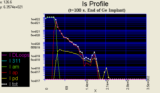
Finally, it is worth pointing out that interstitial concentration in amorphous layer is 1.1 x 1022 cm-3 approximately, as can be seen in previous graphic. Vacancy concentration is basically the same. Therefore, the total amount is the amorphization threshold.
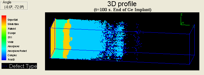
Next, it is shown a very clear view of the profile at 100 s in three dimensions. It is interesting to notice the crystalline/amorphous interface which is well shown in this image. A high amorphous pocket density can be seen beyond that interface.
![]()
Once the Ge implantation finishes, the amorphized region stops growing. Next, anneal begins and the recrystallization starts to clean all defects. The crystalline/amorphous interface sweeps the amorphized region towards the surface, cleaning I and V defects and leaving behind a crystalline Si lattice. At the other side of the crystalline/amorphous interface, however, damage must be annealed to dissolve all defects (EOR Defects).
That is why usually implants in Si are preferred to be amorphizing. It is better to amorphize the silicon sample than to obtain some no-amorphized regions with a very high damage concentration.
Next images show the evolution of the recrystallization. When it finishes, the amorphized region has become an almost perfect Si lattice, whereas the damage in the no-amorphized region has only partly dissolved. It is important to notice the speed of the recrystallization. If the temperature is high enough, recrystallization can occur in just one or a few seconds.
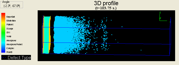
The first two captures are made at 103.5 s. The temperature has already increased considerably and recrystallization has just started, so amorphous layer thickness is reducing continuously.
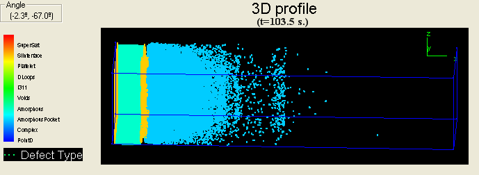

In the non-amorphized region, amorphous pockets have dissolved slightly and {311} defects start to grow. The following captures are made at 103.75 s and the recrystallization is about to finish. The Si amorphous layer has been almost recrystallized completely and I and V damage has been cleaned.

![]()
As it has been stated, the Si region beyond the initial crystalline/amorphous interface, which is below the amorphization threshold level, does not amorphizes. However, defects (EOR) in this region are in a very high concentration. Its name is due to its location along the silicon bar: they are just next to the amorphized region or, in other words, they are at the end of the amorphization range.
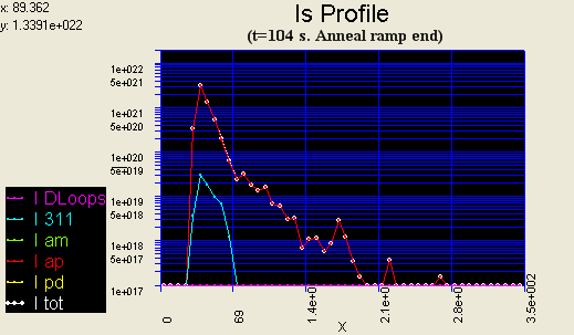
In this region, when the 800 °C anneal starts, EOR defects starts to evolve. After the anneal ramp, all the point defects are grouped in amorphous pockets and internal recombination within them has taken place. When recrystallization finishes, interstitial concentration is still high. Next graph shows the interstitials profile at 104 s. Most of them are in amorphous pockets, and some {311} have already appeared.
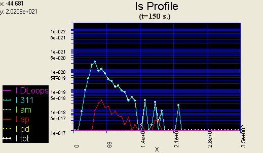
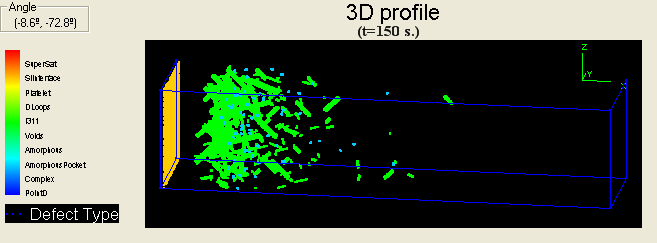
During anneal, the Ostwald ripening process begins: big amorphous pockets are increasingly big, whereas the small ones are increasingly small. The main reason is that, in general, big amorphous pockets are more stable than small ones.
When amorphous pockets are big enough, they evolve into a more stable form: {311} defects. Next graphs shows a snapshot at 150 s: {311} defects are predominant and amorphous pockets are about to dissolve.
Then, {311} defects continue growing. If the amount of interstitials atoms and the temperature are high enough, {311} defects also evolve into a more stable form of extended defects, the Dislocation Loops. Dislocation Loops are planar and circular defects lying on {111} planes.
The following images show {311} defects dissolution and the formation of several small dislocation loops. The two following snapshots correspond to 340 s.
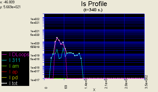
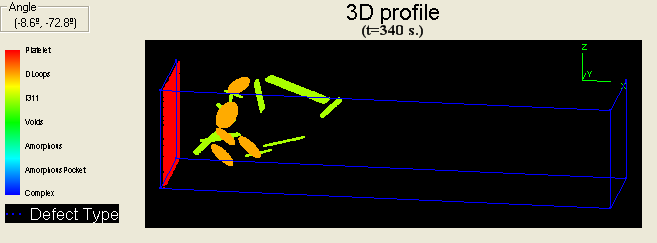
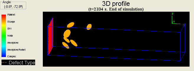
Dislocation loops remain without dissolving at the end of this simulation. A longer anneal would make the dislocation loops to shrink and finally disappear.
![]()
![]() Pelaz L.,
Marqués L. A., and Barbolla J., "Ion-beam-induced amorphization and
recrystallization in silicon". J. Appl. Phys. 96, 5947 (2004)
Pelaz L.,
Marqués L. A., and Barbolla J., "Ion-beam-induced amorphization and
recrystallization in silicon". J. Appl. Phys. 96, 5947 (2004)
![]() Mok K. R.
C., Jaraiz M., Martín-Bragado I., Rubio J. E., Castrillo P., Pinacho R.,
Barbolla J., Srinivasan M.P., "Ion-beam amorphization of semiconductors: A
physical model based on the amorphous pocket population", Journal of Applied
Physics, 98, 046104 (2005)
Mok K. R.
C., Jaraiz M., Martín-Bragado I., Rubio J. E., Castrillo P., Pinacho R.,
Barbolla J., Srinivasan M.P., "Ion-beam amorphization of semiconductors: A
physical model based on the amorphous pocket population", Journal of Applied
Physics, 98, 046104 (2005)
![]() Mok K. R.
C., Colombeau B., Benistant F., Teo R. S.,Yeong S. H., Yang B., Jaraiz M., Chu
S. F. S., "Predictive simulation of advanced Nano-CMOS devices based on kMC
process simulation", IEEE Transactions on Electron Devices 54, 2155
(2007)
Mok K. R.
C., Colombeau B., Benistant F., Teo R. S.,Yeong S. H., Yang B., Jaraiz M., Chu
S. F. S., "Predictive simulation of advanced Nano-CMOS devices based on kMC
process simulation", IEEE Transactions on Electron Devices 54, 2155
(2007)