 daVinci Hardware Guide by
Jesús
Arias.
daVinci Hardware Guide by
Jesús
Arias.
daVinci Hardware Guide by
Jesús
Arias.
(updated: 1999-10-25)
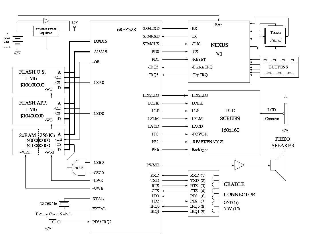
The information contained in this document is the result from a lot of reverse engineering hours into a 2Mb daVinci PDA. This analysis begins with the opening of the PDA to look what's inside, continues with a hardware hack in order to make the serial boot loader of the dragonball processor possible, and concludes with the execution of simple test programs.
Some information comes from the disassembled O.S. code. Following this way Mark Tillotson found the NEXUS chip commands for touch panel and buttons. The O.S. boot section is also very interesting in order to identify general pourpose I/O pins and memory mapping.
Other data like cradle connector pins and schematic is freely available on Internet.
This documentation may be erroneous and/or inaccurate. Use with care.
The "MC68EZ328 Integrated Processor User's Manual" from Motorola is mandatory in order to understand this document.
Contents:
General daVinci schematic.
Memory The LCD. The Nexus Chip.
(2000-06-23) Experimenrtal OS for dragonball daVinci's. (Spanish only)
(1999-10-25) Nexus Power Down. Power Measurements.
(1999-10-24) PF0 & PD1 pin functions.
Two daVinci models are known to this date: The 256K and the 2Mb. The total amount of memory of each model is:
256K: 256 Kb RAM, 1MB Flash.
2Mb: 256 Kb RAM, 2MB Flash.
As you can note the first model is named by RAM and the second by Flash. This is obviously a marketing strategy, but i personally think it's just a lie.
The daVinci O.S. maps it's memory via 68ez328 programmable chip selects. The particular memory address are the same used in the Palm Pilot. What do you think about it?
PRIMARY FLASH $10C00000 (1 Mb)
SECONDARY FLASH $10400000 (1 Mb)
RAM $00000000 (Only the first 64 Kb) $10000000 (The whole 256 Kb)
The RAM memory is implemented by two Hyundai HY62V8100A chips. Each Chip has 128K, 8 bit wide, memory cells. The 68ez328 is configured to use a 16 bit data bus, so each RAM chip fills half data bus. One chip is connected to D0-D7, while the other is connected to D8-D15.
One interesting aspect of the RAM is the double mapping. This is possible thanks to the use of two 68ez328 chip select outputs that are or'ed together by means of one external 74hc08 gate. The Chip Select outputs are:
CSB0: Base=$10000000 Size=256Kb Wait_States=0 Read_Only=NO Supervisor_Only=NO Bus_Width=16 bits
CSC0: Base=$00000000 Size=64Kb Wait_States=0 Read_Only=NO Supervisor_Only=NO Bus_Width=16 bits.
There are two 1Mb flash chips in the 2Mb daVinci version or only one in the 256K. These chips have their part number intentionally erased, but the pin count shows that they mush be 16 bits wide. Anyway, all the modern memory chips can be identified by software, and the daVinci Flash yields the following ID numbers:
Manufacturer ID: $0004 (Fujitsu)
Device ID: $225B (MBM29LV800BA)
These Flash can protect each sector individually. When protected, one sector cannot be programmed or erased without the application of high voltage (12 V) at the reset pin, and executing a previous unprotect command, while unprotected sectors can be erased or programed at only 3.3 volts. The primary Flash has it's first 3 sectors protected (32 Kb). This memory area contains the daVinci boot code. The rest of the primary flash (O.S.), and the whole secondary flash (App's) are unprotected.
The primary Flash is selected via CSA0, the default boot chip select. The Secondary Flash is selected via CSD0. The programming of these chip selects are:
CSA0: Base=$10C00000 Size=1Mb Wait_States=1 Read_Only=NO Supervisor_Only=NO Bus_Width=16 bits Flash_Timming=NO
CSD0: Base=$10400000 Size=1Mb Wait_States=1 Read_Only=NO Supervisor_Only=NO Bus_Width=16 bits Flash_Timming=NO
Notes:
The LCD controller has a direct connection to the 68ez328. The main aspects are:
The LCD screen can display grayscale images with 2 & 4 bit/pixel. These modes are programed via "LCD Panel Interface Configuration Register". The only problem with grayscale modes is the flickering, that can be eliminated programing a faster pixel clock in the "LCD Pixel Clock Divider Register". The default divider value is 6, that is good for Black&White images. For 2 & 4 bit/pixel modes the divider must be 3 and 1 respectively.
The daVinci includes a custom chip that handles the touch panel and buttons. This chip is labeled "NEXUS rev 1.0", and connects to the 68ez328 via the Serial Peripheral Interface (SPI).
The SPI is a bi-directional interface. While one bit is shifted out trough SPIMTXD, another bit is shifted in from SPIMRXD. The timing is controlled with SPIMCLK. From the NEXUS chip this means that you can send commands to the NEXUS while reading previous data.
The SPI clock is programed to a very low rate (sysclock/512 = 32384 Hz). This provides time enough to perform A/D conversions while moving data. The Phase & Polarity of the clock are programmed to the default value "00". The transfers are 10 bits long. Before any transfer the select pin of the NEXUS chip must be driven low via the general pourpose i/o pin PD0. A delay of more than 50 usec between PD0 assertion and SPI data transfer must be done by software for proper operation.
The PD1 I/O pin is probably connected to NEXUS reset, because it must be high for proper operation.
Reading
touch panel coordinates.
| TRANSFER | SPI WRITE | SPI READ |
|
|
|
|
|
|
|
|
|
|
|
|
X & Y coordinates are obtained from a 10 bit A/D converter, so they are in the [0-1023] range.
|
|
|
|
|
|
|
|
|
|
|
|
BUTTONS is a 10 bit word. The pressed buttons are read as 0. The button
mapping is:
|
|
|
|
|
|
|
|
|
|
|
|
|
|
|
|
|
|
|
|
|
|
|
|
|
|
|
|
|
|
|
|
|
|
|
|
The actual voltage is Vbat*3.3/1024
The Nexus chip allows a command to reduce power
requirements when the daVinci is sleeping. For proper power-down a delay
between the last valid Nexus command and the actual power-down command
is required.
| TRANSFER | SPI WRITE | SPI READ |
|
|
|
|
The NEXUS chip post an interrupt to the 68ez328 when a button is pressed or a tap is done on the touch panel:
The daVinci cradle connector is a PCB edge type with 12 signals. 4 lines are intended for serial communications, 3 for the external keyboard, 1 for a reserved interrupt input, 2 for power, and 2 are unconnected. All the signals uses CMOS logic levels (0 volt for FALSE, 3.3 volt for TRUE)
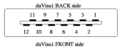
| Pin
Number |
Signal
Name |
Description | Direction
with respect to daVinci |
Functionality |
| 1 | RxD | Data
Receive |
Input | Serial data in. Up to 115200 baud. |
| 2 | TxD | Data
Transmit |
Output | Serial data out. Up to 115200 baud. |
| 3 | RTS | Request to
Send |
Output | daVinci asserts RTS when it is
ready for host data. (not connected to PC) |
| 4 | CTS | Clear to
Send |
Input | Host asserts CTS when it is
ready for daVinci data. (not connected to PC) |
| 5 | GND
(Vss) |
Ground | Power | 0 Volts |
| 6 | PD3 | Keyboard | Input | Data input from keyboard |
| 7 | PD2 | Keyboard | ? | Clock for keyboard |
| 8 | IRQ6 | Reserved | Input | Reserved Interrupt input |
| 9 | IRQ1 | Keyboard | Input | Keyboard Interrupt |
| 10 | Vcc
(Vdd) |
Power | Power | 3.3 Volts |
| 11 | NC | - | - | Not connected (reserved) |
| 12 | NC | - | - | Not connected (reserved) |
Cradle Schematic. (postscript version).
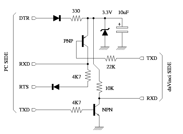
As one can see from the above schematic, the PC must provide the power for logic level conversion via DTR & RTS pins. For proper operation DTR must be high (1 in 16550 MCR) and RTS low (0 in 16550 MCR). With this circuit the actual RS232 levels are +3.3 and -12 Volts. A little low H level, but still high enough for proper operation. Note that no current is drawn from the daVinci side, so serial communications only have a little impact on battery lifetime. The daVinci TXD pin can be configured as OPEN DRAIN output with PULL-UP or TOTEM POLE output.
The only way to produce sound in the daVinci is it's piezoelectric speaker. This speaker is connected to PWMO output, probably trough a single transistor voltage amplifier. The quality of this sound system is so poor that it can only be intended to produce beeps.
The poor characteristics of the sound system are due to the resonant nature of the piezoelectric speaker, the absence of anti-alias filters, and probably to the non-linearity of the amplifier. Although the PWMO output of the 68ez328 can play 8 bit samples at rates up to 8, 16 or 32 KHz, the big distortions makes this potential feature useless, as the following test shows:
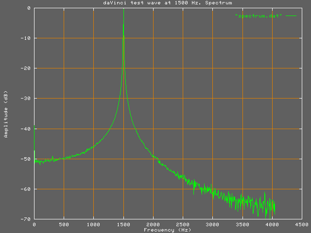
A synthesized 1500 Hz sine wave was played trough the PWMO output at 32384 Hz sampling rate with 4 times sample repeating. This makes an effective 8096 Hz sampling rate while the PWM carrier is at 32 KHz. The sampled & quantized wave is:
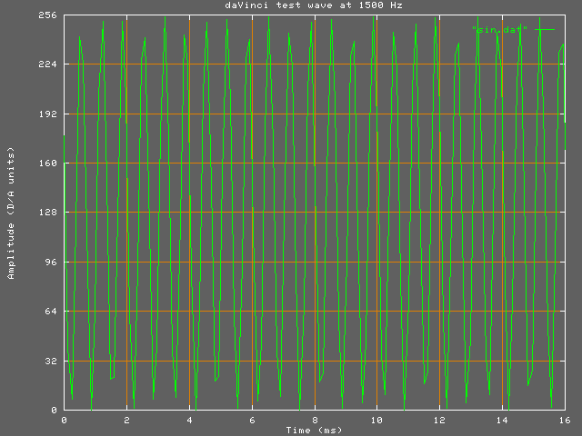
The low sampling rate makes the wave a little irregular, but looking at the spectrum we can see that this wave is a very "monochromatic" sound:
The sound that actually emits the daVinci has the following spectrum:
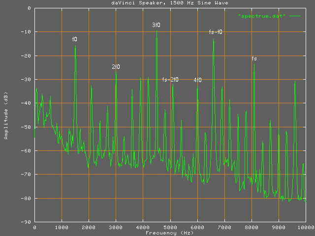
In this graph we remark the fundamental 1500 Hz frequency (f0), it's harmonics (2f0, 3f0,...), the 8096 Hz sampling frequency (fs) and some alias frequencies (fs-f0, fs-2f0,...). As we can see, the spectrum of the played sample is very different from the expected single tone output. We can also note that the third harmonic is the strongest signal. The conclusion is:
The daVinci is unable to play sampled waves. It can only play simple square or rectangular waves. This limitation is due to the sound amplifier and speaker, not to the dragonball processor.
The daVinci has a little switch on it's rear that locks the battery cover. This switch must be pulled-up in order to replace the batteries. One usually don't suspect that this switch has software implications. But a simple test shows that this switch pulls PD5 low when unlocked. This pin has interrupt capabilities, so, when you unlock the battery cover a level 2 interrupt is posted to the core and the O.S. can do some "urgent" processing before the battery removal.
The following table shows the magnitude of the
power requirements for some different daVinci conditions. The measurements
were taken while the CPU executes a do_nothing_loop().
|
|
|
| CPU Full Speed (16.5 MHz), LCD ON, BACKLIGHT ON |
|
| CPU Full Speed (16.5 MHz), LCD ON |
|
| CPU Full Speed (16.5 MHz), LCD OFF |
|
| CPU doze mode 1/32, LCD OFF |
|
| CPU doze mode 0/32 (stopped), LCD OFF |
|
| PLL OFF, LCD OFF |
|
| PLL OFF, LCD OFF, Nexus Power-Down |
|
From the above table we can derive the current
needed for each subsystem:
|
|
Current (mA) |
| Nexus Chip |
|
| LCD |
|
| Backlight |
|
| CPU at Full Speed (16.5MHz) |
|
| CPU, doze mode: N/32 |
|
| CPU Peripherals & PLL system |
|